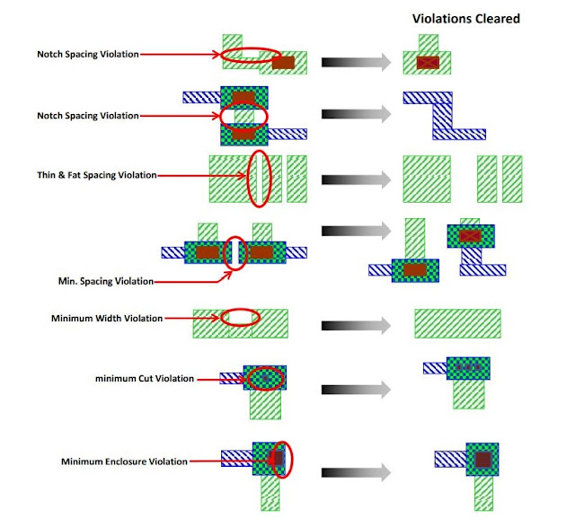
Physical Verification, also known as sign-off verification, is a critical step in the design process for integrated circuits. Physical verification is the process of verifying that the layout of a digital circuit meets the design rules and manufacturing requirements. Physical verification ensures that the design can be manufactured with high yield and reliability.
The physical verification process involves several steps, including design rule checking (DRC), layout versus schematic (LVS) checking, and electrical rule checking (ERC). DRC checks the layout against a set of design rules that specify the minimum feature size, spacing, and alignment requirements. LVS compares the layout with the schematic and verifies that the layout matches the intended design. ERC checks the layout against a set of electrical rules that ensure that the circuit operates correctly and reliably.
The physical verification process also includes layout optimization and analysis. Layout optimization is the process of adjusting the layout to improve its manufacturability, yield, and reliability. Layout analysis is the process of evaluating the layout to identify potential issues, such as parasitic effects, that could affect the performance of the circuit.
Physical verification is critical because it ensures that the circuit can be manufactured with high yield and reliability. Physical verification catches errors and issues that may not be caught during the design phase. Physical verification also ensures that the circuit operates correctly and reliably under real-world conditions.
Physical verification is typically carried out using specialized software tools that are specifically designed for this purpose. These tools perform DRC, LVS, ERC, and layout analysis. The physical verification process requires expertise in semiconductor manufacturing, layout design, and electrical engineering.
In conclusion, physical verification is a critical step in the design process for integrated circuits. Physical verification ensures that the layout of the circuit meets the design rules and manufacturing requirements. Physical verification catches errors and issues that may not be caught during the design phase and ensures that the circuit operates correctly and reliably under real-world conditions. The physical verification process involves several steps, including DRC, LVS, ERC, layout optimization, and analysis. Physical verification requires expertise in semiconductor manufacturing, layout design, and electrical engineering. A thorough and effective physical verification process is essential to ensure the yield, reliability, and performance of integrated circuits.
On this website, we collaboratively try to create learning resources available, to help future-generation engineers and also working professionals in improving their skills in physical verification.
